Basics of DC-DC buck converter
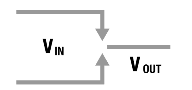
The DC-DC buck converter is a switch-mode step-down converter that provides high efficiency and flexibility at high dropout ratio (VIN) and high load current. The basic circuit is shown in Figure 1. Most Buck converters contain an internal high-side MOSFET and a low-side synchronous rectifier MOSFET switched by an internal duty cycle control circuit to regulate the average output voltage. The waveform at the switching node is filtered by an external LC filter; the output voltage is detected through a feedback loop and the duty cycle of the high-side MOSFET is controlled to achieve voltage regulation. The non-identical device does not have an internal low-side MOSFET and only connects a diode between the external switching node and ground.
The MOSFET is in the turn-off mode, so power consumption is low; and by controlling the duty cycle of the MOSFET, a high dropout ratio (VIN/VOUT) can be achieved. The on-resistance of the internal MOSFET (RDS(ON)) determines the load capability of the buck converter, while the MOSFET’s voltage rating determines its maximum input voltage.
Application current consumption
When considering the rated load current of a DC-DC buck converter, both the average and maximum currents consumed in the application need to be taken into account.
The average current in the application must be lower than the rated load current of the converter, and the difference between the two and the power consumption of the dc-dc buck converter is related to the thermal conditions in the application. This average current will determine the thermal losses of the switching MOSFET, which include the conduction losses and switching losses. The conduction loss is related to the on-state resistance (RDS(ON)) of the internal MOSFET: I2* RDS(ON). If the high-side and low-side RDS(ON) are different, the power consumption of the high-side and low-side MOSFET must also be considered when considering the buck ratio in the application.
The switching losses are related to the current, input voltage, and switching frequency. In general standard applications, the switching losses are about 30% of the total losses; however, in applications with high input voltages or high frequencies, the switching losses increase significantly.
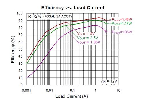
For power supplies used in low power standby mode, it is best to maximize the efficiency of the buck converter at light load. The switching frequency of a forced PWM type buck converter is constant over the full load range. If a high switching frequency is used at light load, most of the losses will be caused by switching losses.